
A logic gate is an elementary building block of a digital circuit. Most logic gates have two inputs and one output. At any given moment, every terminal is in one of the two binaryconditions low (0) or high (1), represented by different voltage levels. The logic state of a terminal can, and generally does, change often, as the circuit processes data. In most logic gates, the low state is approximately zero volts (0 V), while the high state is approximately five volts positive (+5 V).
There are seven basic logic gates: AND, OR, XOR, NOT, NAND, NOR, and XNOR.
The AND gate is so named because, if 0 is called "false" and 1 is called "true," the gate acts in the same way as the logical "and" operator. The following illustration and table show the circuit symbol and logic combinations for an AND gate. (In the symbol, the input terminals are at left and the output terminal is at right.) The output is "true" when both inputs are "true." Otherwise, the output is "false."
![]()
AND gate
| Input 1 | Input 2 | Output |
| 1 | ||
| 1 | ||
| 1 | 1 | 1 |
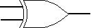
The OR gate gets its name from the fact that it behaves after the fashion of the logical inclusive "or." The output is "true" if either or both of the inputs are "true." If both inputs are "false," then the output is "false."
![]()
OR gate
| Input 1 | Input 2 | Output |
| 1 | 1 | |
| 1 | 1 | |
| 1 | 1 | 1 |
The XOR ( exclusive-OR ) gate acts in the same way as the logical "either/or." The output is "true" if either, but not both, of the inputs are "true." The output is "false" if both inputs are "false" or if both inputs are "true." Another way of looking at this circuit is to observe that the output is 1 if the inputs are different, but 0 if the inputs are the same.
XOR gate
| Input 1 | Input 2 | Output |
| 1 | 1 | |
| 1 | 1 | |
| 1 | 1 |
A logical inverter , sometimes called a NOT gate to differentiate it from other types of electronic inverter devices, has only one input. It reverses the logic state.
![]()
Inverter or NOT gate
| Input | Output |
| 1 | |
| 1 |
The NAND gate operates as an AND gate followed by a NOT gate. It acts in the manner of the logical operation "and" followed by negation. The output is "false" if both inputs are "true." Otherwise, the output is "true."
![]()
NAND gate
| Input 1 | Input 2 | Output |
| 1 | ||
| 1 | 1 | |
| 1 | 1 | |
| 1 | 1 |
The NOR gate is a combination OR gate followed by an inverter. Its output is "true" if both inputs are "false." Otherwise, the output is "false."
![]()
NOR gate
| Input 1 | Input 2 | Output |
| 1 | ||
| 1 | ||
| 1 | ||
| 1 | 1 |
The XNOR (exclusive-NOR) gate is a combination XOR gate followed by an inverter. Its output is "true" if the inputs are the same, and"false" if the inputs are different.
![]()
XNOR gate
| Input 1 | Input 2 | Output |
| 1 | ||
| 1 | ||
| 1 | ||
| 1 | 1 | 1 |
Using combinations of logic gates, complex operations can be performed. In theory, there is no limit to the number of gates that can be arrayed together in a single device. But in practice, there is a limit to the number of gates that can be packed into a given physical space. Arrays of logic gates are found in digital integrated circuits (ICs). As IC technology advances, the required physical volume for each individual logic gate decreases and digital devices of the same or smaller size become capable of performing ever-more-complicated operations at ever-increasing speeds.
See an introductory tutorial on logic gates:
http://whatis.techtarget.com/definition/logic-gate-AND-OR-XOR-NOT-NAND-NOR-and-XNOR


相关推荐
研究了半导体激光器混沌耦合同步及其在光学逻辑门的应用。利用两个混沌半导体激光器的耦合,构建了基本全光...具体提出了全光XNOR、NOR、NOT、组合光电NOR逻辑门及逻辑计算方法,数值模拟结果证明了系统方案的可行性。
Theoretical investigation of phase-based all-optical NOT, XOR and XNOR logic gates based on AlGaAs microring resonators
BP网络实现XOR AND OR逻辑,较具有通用性。
其次,布尔代数使用逻辑运算符,例如合取(and)表示为∧,析取(or)表示为∨,否定(not)表示为¬。 另一方面,初等代数使用算术运算符,例如加法、乘法、减法和除法。 因此,布尔代数是描述逻辑运算的一种形式...
它们是 ADD、SUB、AND、OR、XOR、NOT、SRA 和 SLL。其中 ADD、SUB、AND、OR、XOR 和 NOT 指令具有三地址格式。这些指令的汇编级语法是Opcode rd, rs, rt 其中15-12为指令,11-8为寄存器rd,7-4为寄存器1,3-0为...
很多问题都是课本上没有提及到的 36、给一个表达式f=xxxx+xxxx+xxxxx+xxxx用最少数量的与非门实现(实际上...1)INV 2)AND 3)OR 4)NAND 5)NOR 6)XOR 答案:NAND(未知) 39、用与非门等设计全加法器。(华为)
分立元件的AND、OR和NOT功能都相对简单明确,但XOR和XNOR功能通常需要多个AND、OR和NOT基础功能的组合。 本例给出了一种不常见方法,用两只电阻、四只二极管和一只晶体管,就能完成异或功能。NPN结构获得的是XNOR...
本例给出了一种不常见方法,用两只电阻、四只二极管和一只晶体管,就能完成异或功能。NPN结构获得的是XNOR运算,而PNP结构则得到XOR运算。
北航计算机组成课程设计 支持50条指令的流水线CPU的Verilog代码实现,内包含源代码和相应的测试文件
内置的多输入门如下:and nand nor or xor xnor 这些逻辑门只有单个输出,1个或多个输入。多输入门实例语句的语法如下:multiple_input_gate_type[instance_name] (OutputA, Input1, Input2, . . .,InputN);第一个...
this is the vhdl code for exor gate using dataflow modelling
Demonstration of a directed XNOR/XOR optical logic circuit based on silicon Mach-Zehnder interferometer
VHDL例程源码 xor2VHDL例程源码 xor2VHDL例程源码 xor2VHDL例程源码 xor2VHDL例程源码 xor2VHDL例程源码 xor2VHDL例程源码 xor2VHDL例程源码 xor2VHDL例程源码 xor2VHDL例程源码 xor2VHDL例程源码 xor2VHDL例程源码 ...
XOR算法,可用检查自己的计算结果是否正确
一个JAVA源程序,用面向对象方法开发和设计的,JAVA的4种逻辑门的设计AND,OR,NOT,XOR
基于耦合谐振器感应的透明性的XOR / XNOR定向逻辑电路
针对现有的“与/异或”( AND / XOR )复合门级联设计导致的大型,连续长的不足,提出一种基于晶体管级的三输入AND / XOR复合门电路结构 。该电路通过采用多轨结构,扩展传输路径,以及混合CMOS逻辑设计方法,来克服...
三输入高性能AND_XOR复合门电路设计
we should use Intel-FPGA to make code to implement 4 ... In addition we also should use And OR NOT to implement XOR gate.After above we should compile and simulate the code and understand it how to work.
虽然逻辑运算的种类很多,但实际上ALU中的逻辑电路单元通常只处理AND、OR、XOR、NOT这四种运算,其它的各种逻辑运算都可以由布尔代数化简,只需用AND、OR、XOR、NOT这四种运算便可完成。最后,将算术单元电路和逻辑...